who we are
About us
Laboratry for Heterogeneous Integrated Systems Laboratory, Faculty of Science and Engineering, Department of System Design Engineering, Keio University
what do we Research
Imagination is important than knowledge.
– Albert Einstein
We design the energy-efficient compuring system by introducing heterogenious integration technologies such as emering nanoelectronics devices, interconnec technology, 3D integration and cryo-CMOS.
Our research expands from process, device, device modeling, circuit-device interaction, prototype-chip to architecture and algorithm including classic-quantum co-optimization.
research ACTIVITY-1
Multi-level Interconnect System
research ACTIVITY-2
Brains in Silicon
RESEArCH ACTIVITY-3
3D-stacked Chips Cooling System
RESEArCH ACTIVITY-4
Quantum/Classical Hybrid System
where to MEET us
“Alone we can do so little. Together we can do so much.” – Helen Keller
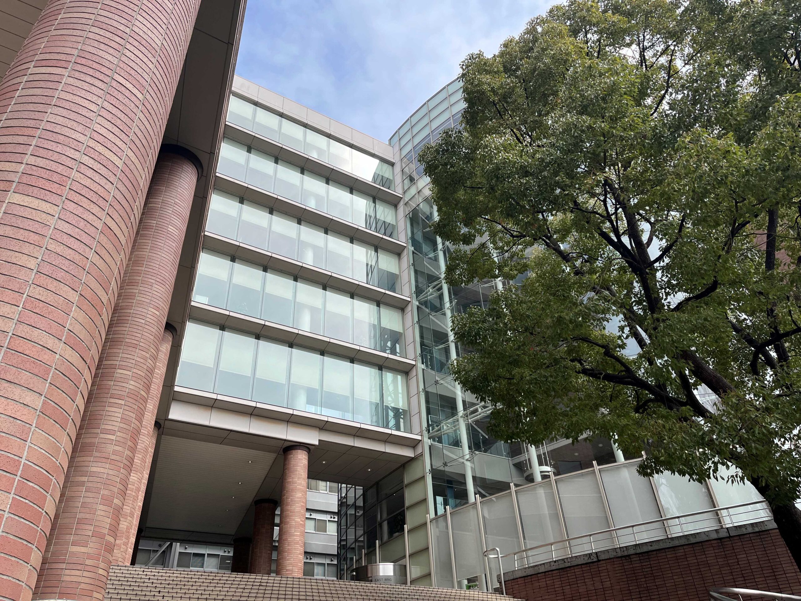
Our lab is located at Keio University, Yagami campus.
Address: 3-14-1, Hiyoshi, Kohoku-ku, Yokohama, Kanagawa 223-8522, Japan
Please visit us by following access.
We are waiting for your active collaboration to love what you do !!

We would love to hear from you!
photo:benzoix/Freepik