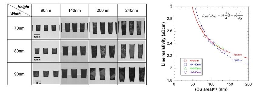
In alignment with the breakdown of technical barriers by transistor technology, facilitating downscaling and transitioning from planar MOS to FinFET, and further to nanosheets, the reduction in size of interconnects has become essential for the scaling.
In traditional aluminum (Al) interconnects, the parasitic resistance of the interconnects significantly started to impede the operational speed of circuits. Since the late 90s, copper (Cu) interconnects, introduced by lower electrical resistivity, took over Aluminum (Al) interconnects. The transition from Al to Cu interconnects is drascitc process changes in the interconnect process, in which represents an innovative shift from Reactive Ion Etching (RIE) process for metal to dielectric, resulting in damascene process. In the damascene process, Cu is vuried in trenches and vias formed by RIE for dielectric films.
Over the last two decades, in response to the trend of scaling, the utilization of copper (Cu) interconnects has expanded with the introduction of various innovative technologies. The operational speed of semiconductor circuits currently mature in the market is considerably constrained by the resistance-capacitance (RC) delay of interconnects. We are focusing on replacing Cu interconnect by emerging metallization technologies that are under development to extend the use of Cu below 1 nm node. Alternative metal interconnect technologies are expected to overcome the limitations of Cu interconnects.

Tada et al., “Feasibility Study of 45-nm-Node Scaled-Down Cu Interconnects With Molecular-Pore-Stacking (MPS) SiOCH Films,” in IEEE Transactions on Electron Devices, vol. 54, no. 4, pp. 797-806, April 2007, doi: 10.1109/TED.2007.892357.